
Working with the screen
I received my 2.4" TFT 40pins ILI9341 screen, together with a board with a FPC connector and pins. Let's see how I made it work (I'll save you my tribulations).
TODO:
- [ ] Check with the screen I did not butcher the actual IM0 IM1 IM2 pinout.
Where to buy the screen ?
I took it from Aliexpress, it was the only one I found which was working in 3.3 for both VDD and VDDI
Here are the photos of the screen on the website, in case the vendor disapears, so you could try a research by picture?
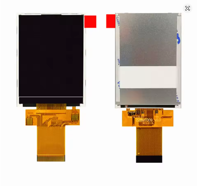
Wiring it to the NucleoF446RE ?
| FPC | FUNCTION | STM32F4 |
|---|---|---|
| 1 | X- (touch) | ignored |
| 2 | Y- (touch) | ignored |
| 3 | X+ (touch) | ignored |
| 4 | Y+ (touch) | ignored |
| 5 | GND | GND |
| 6 | VDDI (2.8-3.3V) | 3.3V |
| 7 | VDD (2.8-3.3V) | 3.3V |
| 8 | NC/FMARK (TE) | ignored |
| 9 | CSX (SPI CS) | GND |
| 10 | DCX (DC,A0) | PB8 |
| 11 | WRX | PB9 |
| 12 | RDX | PB10 |
| 13 | SPI SDI (MOSI) | ignored |
| 14 | SPI SDO (MISO) | ignored |
| 15 | RESX (RESET) | PB12 |
| 16 | GND | GND |
| 17 | DB0 | PC0 |
| 18 | DB1 | PC1 |
| 19 | DB2 | PC2 |
| 20 | DB3 | PC3 |
| 21 | DB4 | PC4 |
| 22 | DB5 | PC5 |
| 23 | DB6 | PC6 |
| 24 | DB7 | PC7 |
| 25 | DB8 | PC8 |
| 26 | DB9 | PC9 |
| 27 | DB10 | PC10 |
| 28 | DB11 | PC11 |
| 29 | DB12 | PC12 |
| 30 | DB13 | PC13 |
| 31 | DB14 | PC14 |
| 32 | DB15 | PC15 |
| 33 | LED-A | 3.3V |
| 34 | LED-K | pulldown 10 ohm |
| 35 | LED-K | pulldown 10 ohm |
| 36 | LED-K | pulldown 10 ohm |
| 37 | GND | GND |
| 38 | IM0 | 3.3V |
| 39 | IM1 | 3.3V |
| 40 | IM2 | GND |
How to communicate with the screen ?
So, as I am using a STM32F4, apparently I could use either DMA (Direct Memory Access) or FSMC(). Claude says FSMC is faster, but he also said I could not use it with my chip (wrong), so I went for DMA, and we'll see annother day if FSMC is faster or not.
The idea is:
- we send the 2 bytes of data for une pixel via D0-D15
- we pulse the WRX pin simultaneously
- we set the DCX pin to 0 for command, 1 for data
- Usually there would be some bit manipulation to get the right bit on the right pins, but since my mapping is direct PC0 to PC15, I can just write the data directly to the GPIO port.
void setupPins() {
   // Control pins
   pinMode(TFT_DC, OUTPUT);
   pinMode(TFT_WR, OUTPUT);
   pinMode(TFT_RST, OUTPUT);
   pinMode(TFT_RD, OUTPUT);

   digitalWrite(TFT_WR, HIGH);
   digitalWrite(TFT_RST, HIGH);
   digitalWrite(TFT_RD, HIGH);

   // Enable GPIO clocks
   RCC->AHB1ENR |= RCC_AHB1ENR_GPIOBEN | RCC_AHB1ENR_GPIOCEN;

   // Set all PC0-PC15 pins to output mode (data bus)
   GPIOC->MODER = 0x55555555;
   // Set all data pins to push-pull, high speed
   GPIOC->OTYPER = 0x0000;     // All push-pull
   GPIOC->OSPEEDR = 0xFFFFFFFF; // All high speed
 }

 inline void pulseWR() {
   GPIOB->BSRR = (1 << (9 + 16));  // WR low (PB9)
   __NOP(); // Small delay
   GPIOB->BSRR = (1 << 9);         // WR high (PB9)
 }

 inline void write16(uint16_t data) {
   // Here there should be some bits manipulation,
   // but my pinout makes it EASY
   GPIOC->ODR = data;
   pulseWR();
 }

 void setBusToInput() {
   GPIOC->MODER = 0x00000000;
 }

 void setBusToOutput() {
   GPIOC->MODER = 0x55555555;
 }

 void writeCommand(uint8_t cmd) {
   digitalWrite(TFT_DC, LOW);
   write16(cmd);
 }

 void writeData(uint8_t data) {
   digitalWrite(TFT_DC, HIGH);
   write16(data);
 }

 void writeData16(uint16_t data) {
   digitalWrite(TFT_DC, HIGH);
   write16(data);
 }
And that's it, you are ready to communicate ! You can browse the full code here, with the inheritance of the Adafruit_GFX class so that you can draw anything easily.